If you have a specialist test requirement, our dedicated team can design and build a tailor-made test solution for you to ensure that your product meets your exact functional specifications.
Within the company, we use a standardized process to drive improvements for the benefit of our customers. Our multi-disciplined continuous improvement team works to further improve overall performance, saving you precious time and money.
Some of our testing capabilities are:
In-Circuit Test (ICT):
- Test fixture design and procurement
- Test program development
- Boundary Scan
- In-system programming
Final System Test and Configuration
- Test Design
- System level programming and serialization
Functional Test
- In-house fixture design and development
Burn-in
- Thermal cycling
- Power cycling
- Functional and system-level testing
Inspection:
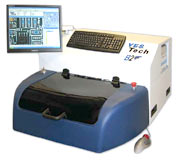
Using Yestech Latest Automated Optical Inspection machine capable of detecting components as small as 0201 packages to QFP and through hole components.
Repair Services:
We offer a range of repair services ranging from product upgrades, engineering changes, component recovery, memory module and BGA repairs using conceptronic freedom 2000 Rework Station.
The machine will detect component position, missing, wrong polarity, skew, and tombstone. Lead detected if bent, lifted and bridging. Solder quality includes open insufficient, Short and solder ball.
X-Ray Inspection
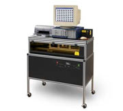
Using the Glenboork xray machine to inspect PCB and assemble boards containg BGAs, uBGAs and Flip Chips
- AOI
- X-Ray
Cygnus Uses Optical Inspection on all production boards to ensure to check components missing, shorts, open orientation and solder quality.
YTV B2 AOI
Tabletop Automated Optical Inspection
- Quick Set-up
- Color Camera
- High Defect Coverage
- Low False Failure Rate
- Best Price Performance

YESTech’s advanced Thin CameraT technology offers off-line tabletop PCB inspection with exceptional defect coverage. This table-top system inspects solder joints and verifies correct part assembly enabling users to improve quality and increase throughput.
Programming the B2 is fast and intuitive. Operators typically take less than 30 minutes to create a complete inspection program including solder inspection.
- Quick Set-up
- Mega-pixel Color Camera
- High Defect Coverage
- Low False Failure Rate
- Best Price Performance
YESTech’s advanced Thin Camera™ technology offers off-line tabletop PCB inspection with
exceptional defect coverage. This table-top system inspects solder joints and verifies
correct part assembly enabling users to improve quality and increase throughput.
Programming the B2 is fast and intuitive.
Operators typically take less than 30 minutes to create a complete inspection program
including solder inspection. The B2 utilizes a standard package library to simplify training and insure program portability across manufacturing lines. Programs created with the B2 are also compatible with YESTech’s complete line of AOI systems.
Newly available image processing technology integrates several techniques, including color, normalized correlation and rule-base algorithms, to provide complete inspection coverage with an extremely low false failure rate.
The B2 is equally effective for pre / post-reflow or even final assembly inspection. Remote programming maximizes machine utilization and real-time SPC monitoring provides a valuable yield enhancement solution.
Automated Inspection for:
- Solder & lead defects
- Component presence and position
- Correct part
- Polarity
- Through-hole parts
- Paste

The RTX-113 is a unique X-ray inspection system,designed for rapid, reliable inspection of both multi-layer and assembled printed circuit boards.
The RTX-113 is designed for heavy production environments where X-ray is used to inspect PCBs and assembled PCBs containing advanced components such as BGAs, uBGAs and Flip Chips.The system is very versatile and features generates high-resolution, high-sensitivity images, revealing defects as small as 0.001 inch with a full one inch diameter field of view.
Applications:
- Multi-layer PCBs
- Small Hole Drilling
- BGA Inspection
- Backplane Boards

