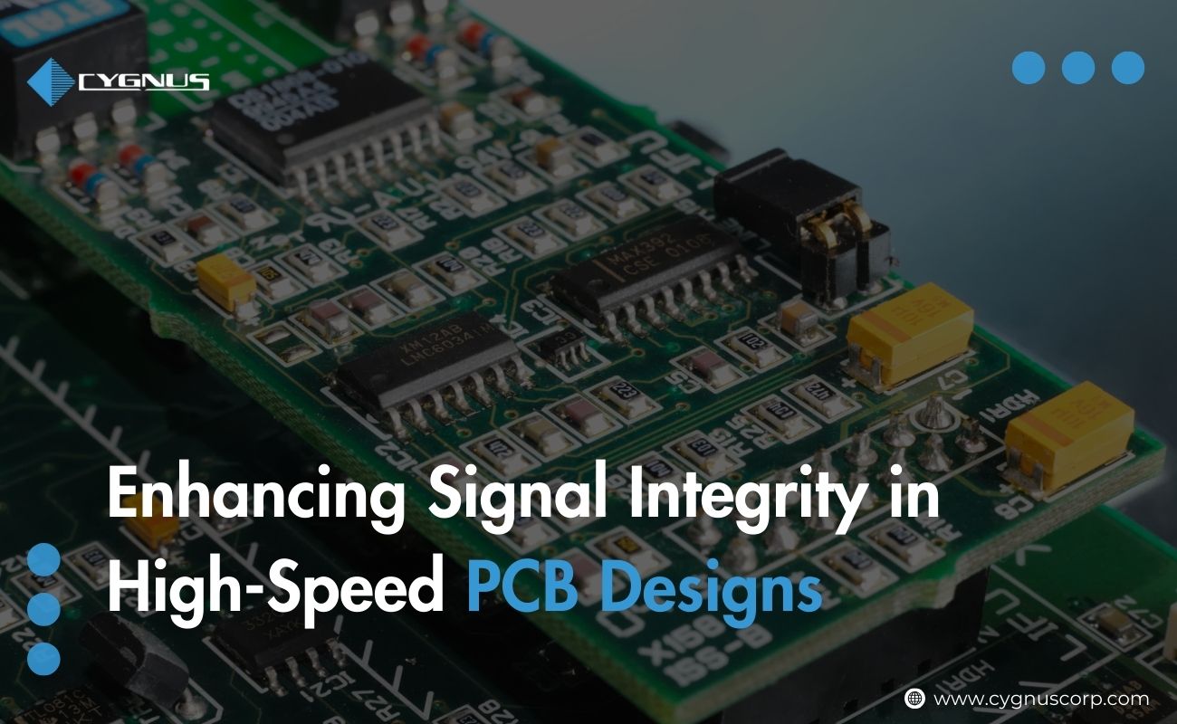
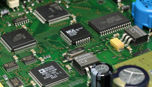
High-speed PCB design is the backbone of modern electronics, powering everything from advanced computing systems to 5G networks. But did you know that poor signal integrity can cause up to 50% of high-speed PCB failures? As data transmission speeds increase, so do the challenges of maintaining signal integrity in high-speed PCB designs. Crosstalk, impedance mismatches, and electromagnetic interference (EMI) can lead to data loss, signal distortion, and reduced performance, issues that engineers can’t afford to ignore.
Signal integrity analysis becoming an important part of PCB development, designers need to implement strategic layout techniques, optimized routing, and high-quality materials to ensure seamless performance. In this blog, we’ll explore the key factors affecting signal integrity in high-speed PCB designs and the best practices to overcome these challenges for reliable and efficient circuit performance.
What is Signal Integrity in High-Speed PCB Designs?
Signal integrity in high-speed PCB designs refers to the ability of electrical signals to travel through a circuit without distortion, interference, or loss of data. As circuits operate at higher frequencies and faster switching speeds, maintaining clean and reliable signals becomes increasingly challenging.
In a high-speed PCB design, signals can be affected by factors like crosstalk, impedance mismatches, and electromagnetic interference (EMI). These issues can lead to delayed transmissions, data corruption, or even complete circuit failure. This is why signal integrity analysis is crucial—it helps engineers identify potential signal issues early in the design phase, ensuring the PCB performs efficiently under real-world conditions.
Key Factors Affecting Signal Integrity:
The table below outlines the key factors that influence signal integrity in high-speed PCB layout and how they impact overall circuit performance.
| Factor | Description | Impact on Signal Integrity |
| Impedance Matching in PCB | Ensuring consistent impedance along signal traces to prevent reflections. | Reduces signal distortion and enhances transmission efficiency. |
| Crosstalk | Unwanted interference between adjacent traces due to electromagnetic coupling. | Can cause noise, signal distortion, and data corruption. |
| Electromagnetic Interference (EMI) | External and internal noise affecting signal transmission. | Leads to degraded performance and potential compliance failures. |
| Propagation Delay & Timing Skew | Variations in signal travel time across PCB traces. | Causes synchronization issues in high-speed circuits. |
| Power Integrity | Stable and clean power distribution across the PCB. | Minimizes voltage fluctuations that can impact signal stability. |
| Trace Routing in High-Speed PCB Layout | Proper routing techniques such as controlled impedance and differential signaling. | Prevents reflections, reduces EMI, and improves signal transmission. |
By optimizing high-speed PCB layout and implementing impedance matching in PCB, designers can significantly enhance signal integrity, ensuring reliable and efficient electronic performance.
Best Design Practices to Improve Signal Integrity
Maintaining signal integrity in high-speed PCB designs requires careful planning and smart design strategies. Here are some best practices to ensure clean and reliable signals:
Optimizing PCB Layout:
A well-structured high-speed PCB design minimizes signal interference and improves overall performance. Keeping traces short, avoiding sharp bends, and maintaining proper spacing between high-speed signals help reduce issues like crosstalk and reflections.
Effective Grounding and Power Distribution:
Poor grounding can introduce noise, affecting PCB signal integrity. Using a solid ground plane reduces electromagnetic interference (EMI) and ensures a stable power distribution network (PDN), preventing voltage fluctuations that could distort signals.
Shielding and Isolation Techniques:
Electromagnetic interference (EMI) can severely impact signal quality. Using shielding techniques like copper pours, ground planes, and separate signal layers can help isolate sensitive signals from noisy components, improving overall signal integrity analysis.
Use of High-Quality Materials:
Choosing the right PCB material is critical. Low-loss dielectric materials, such as Rogers laminates, provide better performance than standard FR4, reducing signal degradation and ensuring faster, more stable signal transmission.
Signal Termination Techniques:
Signal reflections occur when there’s a mismatch in impedance. Proper termination methods, such as series or parallel resistors, help control reflections and ensure signal stability, which is essential for maintaining signal integrity in high-speed PCB designs.
Simulation and Testing for Signal Integrity Optimization:
In high-speed PCB design, ensuring signal integrity is crucial for reliable performance. Advanced simulation tools, such as HyperLynx and Sigrity, enable designers to predict and mitigate potential issues like crosstalk and electromagnetic interference (EMI) before physical prototyping. These tools facilitate comprehensive signal integrity analysis, allowing for adjustments in the high-speed PCB layout to enhance performance. Studies have shown that utilizing simulation can reduce design iterations by up to 30%, leading to faster time-to-market.
Emerging Trends in Signal Integrity for High-Speed PCBs:
The rapid advancement of technology has led to several emerging trends in maintaining signal integrity in high-speed PCB designs:
- Adoption of Advanced Materials: The use of low-loss dielectric materials, such as PTFE and ceramic-filled laminates, is increasing. These materials minimize signal attenuation and maintain integrity at higher frequencies.
- Integration of AI in Design Processes: Artificial intelligence is being utilized to optimize PCB layouts for signal integrity. AI algorithms can predict potential signal issues and suggest design modifications, enhancing efficiency and performance.
- Focus on Power Integrity: There’s a growing emphasis on the relationship between power integrity and signal integrity. Designers are implementing more robust power distribution networks to ensure stable voltage levels, which is critical for maintaining signal integrity in high-speed designs.
Conclusion:
As electronics continue to evolve, maintaining signal integrity in high-speed PCB designs is more critical than ever. Poor signal management can lead to data loss, noise, and performance failures, making it essential to adopt best design practices. A well-optimized high-speed PCB design, combined with effective shielding, grounding, and impedance matching in PCB, ensures reliable signal transmission and reduced interference. Leveraging signal integrity analysis and advanced simulation tools can help engineers detect and resolve potential issues early in the design phase.
FAQs
Signal integrity refers to the ability of electrical signals to travel without distortion or interference. In high-speed PCB designs, maintaining signal integrity is crucial to prevent data loss, signal degradation, and performance issues.
Common causes include impedance mismatches, crosstalk, electromagnetic interference (EMI), poor grounding, and excessive trace lengths, all of which can lead to signal distortion and data corruption.
Popular tools include HyperLynx, Cadence Sigrity, Ansys SIwave, and Keysight ADS, which help analyze and optimize PCB layouts for better signal performance.
EMI and crosstalk can be minimized by using proper trace spacing, adding ground planes, shielding sensitive signals, and implementing differential signaling techniques to maintain signal integrity.


4 Comments
Akun Binance
Your article helped me a lot, is there any more related content? Thanks!
binance referal code
Your point of view caught my eye and was very interesting. Thanks. I have a question for you. https://accounts.binance.info/ru/register?ref=O9XES6KU
Ustvarite osebni racun
Your point of view caught my eye and was very interesting. Thanks. I have a question for you.
开设Binance账户
Your point of view caught my eye and was very interesting. Thanks. I have a question for you.