







A tiny component standing upright might look harmless but in electronics manufacturing, it’s a silent failure waiting to happen.
Tombstoning in PCB assembly is one of the most frustrating and costly soldering defects in PCB production. It disrupts electrical connections, increases rework, and can even lead to field failures if not caught early.
The good news? It’s preventable if you understand what’s really causing it.
What Is Tombstoning in PCB Assembly?
Tombstoning in SMT is a defect where one end of a surface-mount component lifts off the PCB during soldering, standing vertically like a tombstone. This happens due to uneven solder melting and solder surface tension imbalance, pulling the component upward.
Why Tombstoning Is a Critical SMT Defect?
Not all reflow soldering defects are equal and tombstoning is one of the most damaging.
Here’s why:
- Creates open circuits (no electrical connection)
- Leads to immediate product failure
- Increases inspection and rework costs
- Reduces overall production yield
In high-volume production, even a small percentage of SMT defects tombstoning can translate into thousands in losses.
What Causes Tombstoning in PCB Assembly? (Root Cause Breakdown)?
PCB tombstoning is the key to preventing it.
1. Uneven Solder Paste Deposition:
If one pad has more solder paste than the other:
- It melts differently
- Creates uneven force
- Pulls the component upward
This is one of the most common triggers of a tombstoning defect PCB issue.
2. Imbalanced Heating During Reflow:
During reflow:
- One pad reaches melting temperature first
- The molten solder pulls the component
- The opposite side lifts
This is known as reflow profile tombstoning, and it’s directly linked to temperature inconsistencies.
3. Poor Pad Design for SMT Components:
Incorrect pad design for SMT components creates imbalance:
- Unequal pad sizes
- Poor thermal distribution
- Inconsistent wetting
Design mistakes often go unnoticed but they’re a major cause of tombstoning in PCB assembly.
4. Component Placement Issues:
Misalignment during pick-and-place:
- Reduces contact area
- Increases imbalance during soldering
5. Solder Surface Tension Imbalance:
This is the physics behind tombstoning.
When solder melts:
- Surface tension pulls the component toward the stronger side
- If forces aren’t equal → component lifts
👉 This solder surface tension imbalance is the final trigger that causes tombstoning.
How Tombstoning Happens During Reflow Soldering?
Let’s simplify the process:
- Solder paste begins melting
- One pad melts faster than the other
- Surface tension pulls the component
- Opposite side lifts
- Component stands upright
That’s how tombstoning in SMT happens in seconds.
Components Most Affected by Tombstoning:
Not all components are equally vulnerable.
Most affected:
- Chip resistors
- Capacitors
- Small passive components (0402, 0201, 01005)
The smaller the component, the higher the risk of SMT defects tombstoning.
Tombstoning vs Other Soldering Defects in PCB:
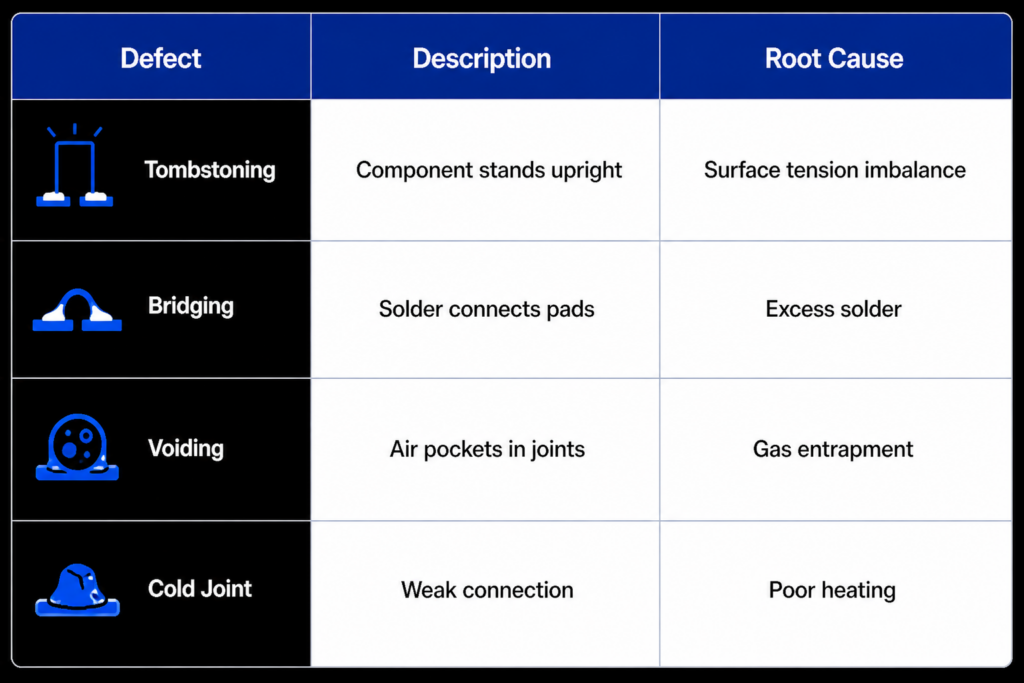
Understanding these differences helps optimize your PCB quality inspection process.
How to Prevent Tombstoning in PCB Assembly?
Now the part that actually saves you money 👇
1. Optimize Solder Paste Printing:
- Ensure equal paste volume
- Use proper stencil design
- Maintain consistent printing process
2. Improve Pad Design for SMT Components:
- Symmetrical pad layout
- Balanced copper areas
- Proper spacing
Good pad design for SMT components eliminates imbalance before production even begins.
3. Control Reflow Temperature Profile:
- Uniform heating across PCB
- Controlled ramp rate
- Proper soak time
Fixing the reflow profile tombstoning issue is one of the most effective solutions.
4. Ensure Accurate Component Placement:
- Calibrate pick-and-place machines
- Maintain alignment precision
5. Use High-Quality Materials:
- Consistent solder paste
- Reliable components
- Stable PCB materials
Best Practices to Reduce Tombstoning in SMT Production:
To truly eliminate tombstoning in PCB assembly, focus on process control:
- Design for manufacturability (DFM)
- Standardized production processes
- Regular inspection checkpoints
- Continuous process monitoring
Prevention is always cheaper than rework.
Real Impact of Tombstoning on Manufacturing (Stats Table):
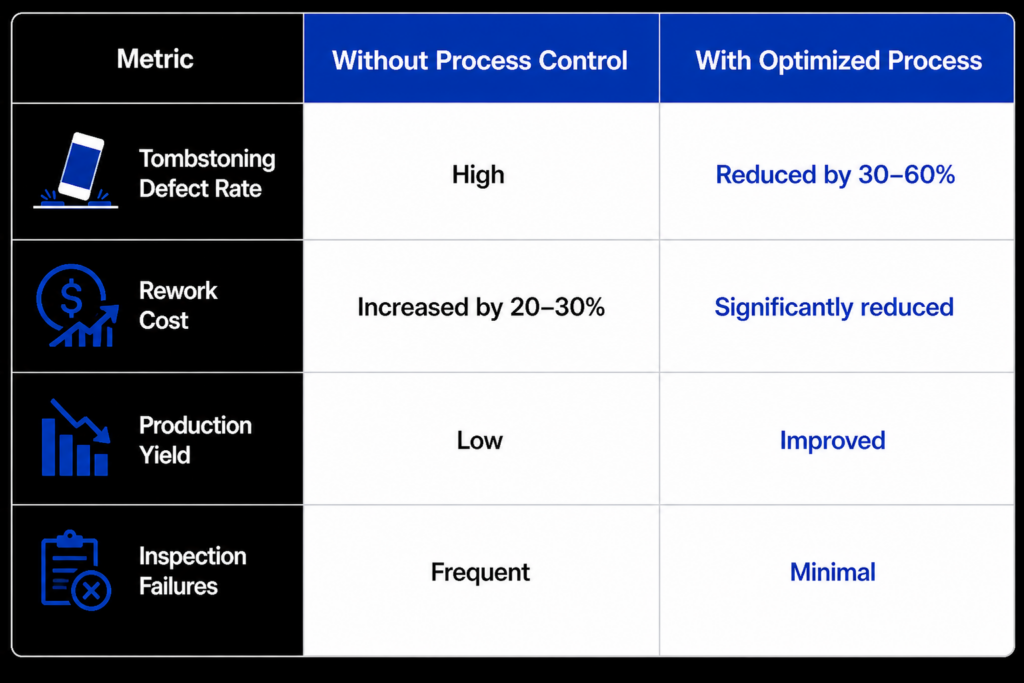
The takeaway: Fixing PCB tombstoning causes directly improves profitability.
How Inspection Helps Detect Tombstoning Early
Even with prevention, inspection is critical.
- AOI (Automated Optical Inspection) quickly detects lifted components
- X-ray confirms solder joint integrity
Together, they ensure no tombstoning defect PCB escapes into the final product.
Build Defect-Free PCB Assemblies with the Right Partner:
Tombstoning isn’t just a defect, it’s a sign that something in your process needs attention.
At Cygnus Electronics, every stage of production from pad design for SMT components to controlled reflow profiles is optimized to eliminate reflow soldering defects like tombstoning.
With advanced inspection, process control, and engineering expertise, Cygnus helps you:
- Reduce defects
- Improve yield
- Deliver reliable electronics
Stop fixing defects later build it right from the start with Cygnus.
Final Takeaway:
If you’re dealing with tombstoning in PCB assembly, the issue isn’t random—it’s systematic.
- Fix the process.
- Balance the design.
- Control the reflow.
Because in SMT manufacturing, even the smallest imbalance…can lift your entire component and your production costs with it.
FAQs
What causes tombstoning in PCB assembly?
Tombstoning is caused by uneven solder paste, imbalanced heating, poor pad design, and solder surface tension imbalance during reflow soldering.
How can tombstoning in SMT be prevented?
It can be prevented by optimizing solder paste deposition, improving pad design, controlling the reflow profile, and ensuring accurate component placement.
Which components are most affected by tombstoning?
Small passive components like chip resistors and capacitors (especially 0402 and 0201 sizes) are most prone to tombstoning.
Is tombstoning a common reflow soldering defect?
Yes, tombstoning in SMT is one of the most common reflow soldering defects, especially in high-density PCB assemblies.