The post Top Reasons for Solder Joint Failure appeared first on Cygnus.
]]>Electronic devices rely on thousands of connections working flawlessly together. While advanced components often receive the most attention, the humble solder joint is what keeps everything connected.
A single failed solder joint can cause intermittent signals, system malfunctions, overheating, or complete product failure. In industries such as automotive, aerospace, telecommunications, and industrial automation, even a minor connection issue can lead to costly downtime and warranty claims.
Understanding the top reasons for solder joint failure helps manufacturers improve reliability, reduce defects, and ensure long-term product performance.
What Is a Solder Joint and Why Does It Matter?
A solder joint is the electrical and mechanical connection created when solder bonds a component lead to a printed circuit board (PCB). These joints allow electrical current to flow between components while also securing them physically to the board.
When properly formed, solder joints provide:
- Reliable electrical conductivity
- Mechanical stability
- Resistance to vibration and thermal stress
- Long-term product reliability
However, when solder joints are poorly formed or exposed to excessive stress, solder joint failure can occur, affecting the performance of the entire system.
Why Solder Joint Failure Is a Major Concern in Electronics Manufacturing?
The reliability of a PCB often depends on the quality of its solder joints. Industry studies have shown that interconnection failures remain one of the leading causes of electronic assembly failures.
Poor solder joints can result in:
- Product recalls
- Increased warranty costs
- Rework and repair expenses
- Production delays
- Customer dissatisfaction
According to manufacturing quality studies, the cost of correcting defects after product shipment can be several times higher than identifying and fixing them during production.
This is why manufacturers invest heavily in PCB assembly quality control, inspection processes, and testing procedures.
Top Reasons for Solder Joint Failure:
The most common causes of solder joint failure can help manufacturers prevent reliability issues before products reach the field.
Cold Solder Joints:
A cold solder joint occurs when solder does not melt or flow properly during assembly.
Common causes include:
- Insufficient soldering temperature
- Improper heating duration
- Poor wetting of surfaces
- Contaminated components
Cold joints often appear dull, rough, or grainy instead of smooth and shiny.
Impact:
- Weak electrical connections
- Intermittent operation
- Increased resistance
- Early product failure
Thermal Cycling and Temperature Stress:
Electronic devices frequently experience temperature changes during operation.
As components heat and cool, materials expand and contract at different rates. Over time, this repeated movement can create microscopic cracks within solder joints.
Industries most affected include:
- Automotive electronics
- Aerospace systems
- Industrial control equipment
- Outdoor communication devices
Thermal cycling is one of the most significant causes of solder joint failure in long-life electronic products.
Poor PCB Design and Component Layout:
Even the best manufacturing process cannot fully compensate for poor design.
Design issues that contribute to solder joint defects include:
- Improper pad sizing
- Uneven copper distribution
- Inadequate thermal relief
- Poor component spacing
Design-for-Manufacturing (DFM) reviews help identify these issues before production begins.
Mechanical Stress and Vibration:
Products exposed to constant movement face additional reliability challenges.
Examples include:
- Automotive control systems
- Industrial machinery
- Transportation electronics
- Aerospace applications
Continuous vibration can weaken solder joints and eventually cause cracking or separation.
The larger and heavier the component, the greater the stress placed on the solder connection.
Insufficient or Excess Solder:
The amount of solder used directly affects joint integrity.
Insufficient Solder:
Can lead to:
- Weak bonding
- Open circuits
- Reduced mechanical strength
Excess Solder:
Can result in:
- Solder bridges
- Electrical shorts
- Inspection failures
These issues are among the most common soldering defects found during PCB assembly.
Flux Residue and Contamination:
Clean surfaces are critical for creating reliable solder joints.
Contamination may come from:
- Dust
- Oils
- Moisture
- Fingerprints
- Residual flux
Contaminants interfere with solder wetting and can eventually cause corrosion.
Over time, contamination-related issues may develop into serious solder joint failure problems.
Voids and Air Pockets:
Voids are trapped air pockets inside a solder joint.
These hidden defects reduce:
- Mechanical strength
- Electrical performance
- Heat dissipation capability
Voids are particularly problematic in:
- Power electronics
- LED assemblies
- High-current applications
Because they are often invisible from the surface, X-Ray inspection is commonly used to detect them.
Lead-Free Solder Challenges:
Environmental regulations have increased the adoption of lead-free solder.
While beneficial for compliance, lead-free alloys present unique challenges:
- Higher processing temperatures
- Increased brittleness
- Greater sensitivity to thermal stress
Manufacturers must carefully optimize soldering processes to maintain reliability.
Common Signs of Solder Joint Failure:
Recognizing failure symptoms early can prevent more extensive damage.
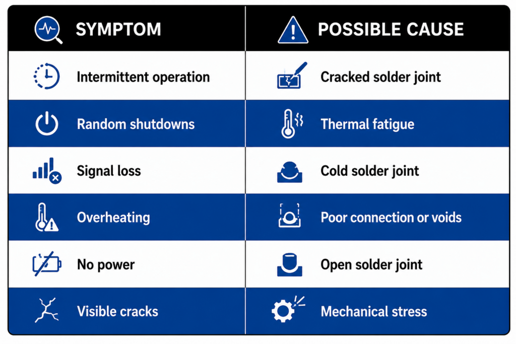
Identifying these warning signs quickly can reduce repair costs and improve product reliability.
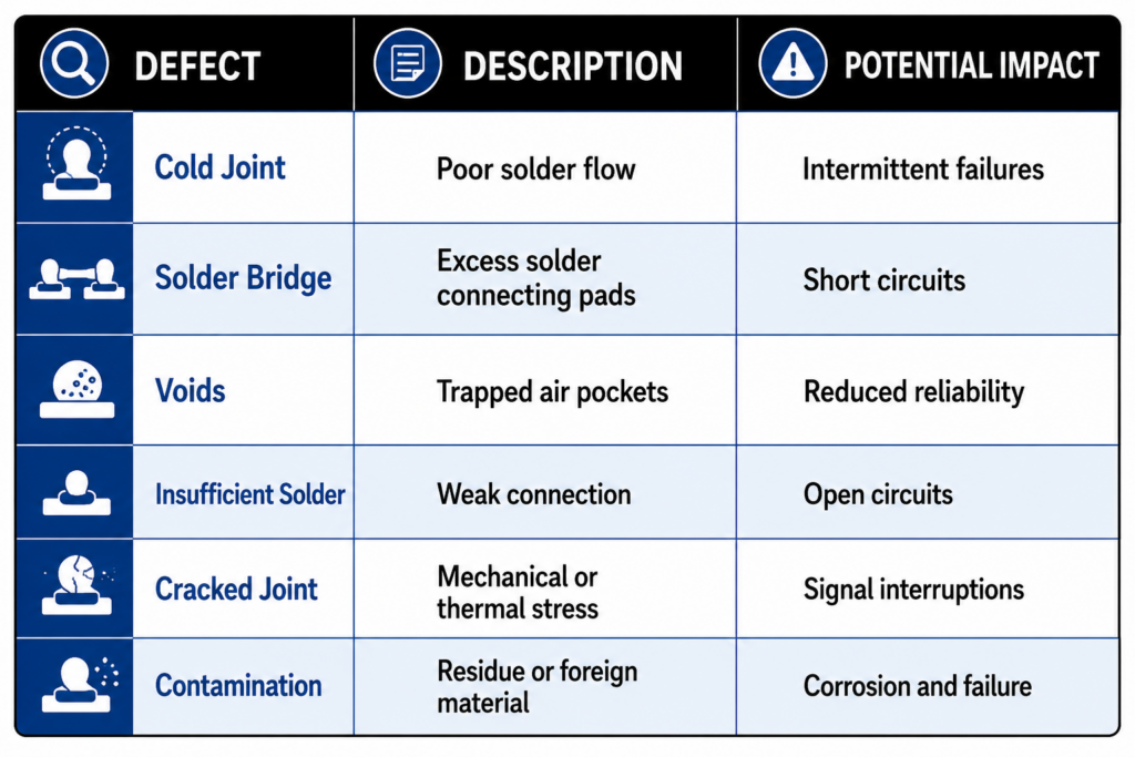
Common Soldering Defects and Their Impact:
The following table summarizes some of the most frequently observed common soldering defects in electronics manufacturing.
How Electronics Manufacturers Prevent Solder Joint Failures?
Preventing defects requires a combination of process control, inspection, and industry best practices.
Process Optimization:
Manufacturers monitor:
- Reflow temperature profiles
- Solder paste quality
- Placement accuracy
- Process consistency
These controls significantly reduce solder joint defects before they occur.
Advanced Inspection:
Quality-focused manufacturers use:
- Automated Optical Inspection (AOI)
- X-Ray Inspection
- Visual Inspection
- Functional Testing
These tools identify defects early in the manufacturing process.
Compliance with IPC Soldering Standards:
Following IPC soldering standards ensures solder joints meet recognized industry requirements for workmanship and reliability.
IPC guidelines provide manufacturers with clear acceptance criteria for:
- Joint appearance
- Solder coverage
- Defect classification
- Inspection requirements
Compliance with IPC soldering standards helps improve consistency across production runs.
The Role of PCB Assembly Quality Control:
Strong PCB assembly quality control programs are essential for preventing defects and maintaining product reliability.
Effective quality control includes:
- Incoming material inspection
- Process monitoring
- AOI verification
- X-Ray analysis
- Functional testing
- Root cause analysis
When combined, these processes dramatically reduce manufacturing defects and improve product performance.
Simply put, quality is not inspected into a product it is built into the process.
Why Choosing the Right EMS Partner Matters?
Reliable solder joints don’t happen by chance.
They result from:
- Experienced engineering teams
- Controlled manufacturing processes
- Advanced inspection technologies
- Continuous quality improvement
An experienced Electronics Manufacturing Services (EMS) provider understands how to identify potential risks before they become costly failures.
By prioritizing PCB assembly quality control, adhering to IPC soldering standards, and utilizing advanced testing methods, manufacturers can significantly improve product reliability and reduce field failures.
Conclusion:
Solder joints may be small, but their impact on product performance is enormous.
The top reasons for solder joint failure include cold solder joints, thermal cycling, contamination, mechanical stress, insufficient solder, voids, and poor design practices. Fortunately, most of these issues are preventable through proper engineering, process control, inspection, and testing.
At Cygnus Electronics, we help OEMs and manufacturers improve product reliability through precision PCB assembly, advanced inspection technologies, rigorous testing, and industry-leading quality assurance practices. Whether you’re building prototypes or scaling production, our team is committed to delivering electronic assemblies that perform reliably in the real world.
Contact Cygnus Electronics today to discuss your next manufacturing project.
The post Top Reasons for Solder Joint Failure appeared first on Cygnus.
]]>The post AOI vs X-Ray Inspection: Which Meets IPC Standards Better? appeared first on Cygnus.
]]>According to IPC, poor solder connections remain one of the leading causes of electronic assembly failures. Studies have shown that manufacturing defects account for a significant percentage of field failures, making inspection a critical part of the production process.
This raises an important question for manufacturers: when it comes to IPC compliance, which inspection method performs better: Automated Optical Inspection (AOI) or X-Ray inspection?
In this guide, we’ll compare AOI vs X-Ray inspection, explain how each technology works, and determine how they contribute to meeting IPC quality requirements.
Understanding IPC Standards in PCB Inspection:
The electronics industry relies on IPC standards to establish consistent quality and workmanship requirements for printed circuit board assemblies.
Some of the most commonly referenced standards include:
- IPC-A-610 (Acceptability of Electronic Assemblies)
- IPC J-STD-001 (Requirements for Soldered Electrical and Electronic Assemblies)
- IPC-7711/7721 (Rework and Repair Standards)
These standards define what constitutes an acceptable solder joint, component placement, and assembly quality.
Effective IPC standards PCB inspection processes help manufacturers:
- Improve product reliability
- Reduce defect rates
- Minimize rework costs
- Meet customer and regulatory requirements
Whether using AOI, X-Ray, or both, the ultimate goal is ensuring products comply with these quality benchmarks.
What Is AOI (Automated Optical Inspection)?
Automated Optical Inspection uses high-resolution cameras and advanced imaging software to inspect printed circuit boards during production.
The system compares captured images against predefined standards or reference models to identify visible defects.
Common Defects AOI Can Detect:
AOI is highly effective at identifying:
- Missing components
- Incorrect component placement
- Wrong component orientation
- Solder bridges
- Insufficient solder
- Polarity issues
Because AOI can inspect boards quickly, it is widely used in high-volume manufacturing environments.
Advantages of AOI:
Fast Inspection Speed:
AOI systems can inspect thousands of solder joints within minutes, making them ideal for production lines.
Early Defect Detection:
Problems can be identified immediately after assembly, reducing downstream failures.
Cost-Effective Quality Control:
Compared to more advanced inspection technologies, AOI offers lower operating costs.
Limitations of AOI:
Despite its advantages, AOI only evaluates visible areas of a board.
It cannot inspect:
- Hidden solder joints
- Internal component connections
- Ball Grid Array (BGA) solder balls beneath packages
As PCB designs continue to evolve, these limitations become increasingly important.
What Is X-Ray Inspection?
Unlike AOI, X-Ray inspection uses electromagnetic radiation to create images of internal structures that cannot be seen from the surface.
This makes X-Ray inspection electronics manufacturing particularly valuable for modern assemblies that contain hidden connections.
Common Defects X-Ray Can Detect:
X-Ray systems can identify:
- BGA solder joint defects
- Voids within solder joints
- Hidden bridging
- Misaligned internal connections
- Insufficient solder beneath components
Because the inspection is non-destructive, manufacturers can analyze internal structures without damaging the board.
Advantages of X-Ray Inspection:
Visibility Beneath Components:
One of the biggest strengths of X-Ray inspection electronics manufacturing is the ability to inspect hidden solder joints.
Superior BGA Analysis:
As BGA packages become more common, X-Ray provides a reliable method for verifying connection quality.
Enhanced Quality Assurance:
Manufacturers gain deeper insight into assembly quality, reducing the risk of defects escaping into the field.
Limitations of X-Ray:
While powerful, X-Ray inspection typically involves:
- Higher equipment costs
- Slower inspection times
- Specialized training requirements
For this reason, many manufacturers use X-Ray strategically rather than on every board.
Also Read: IPC Standards for Solder Joint Quality Explained Simply
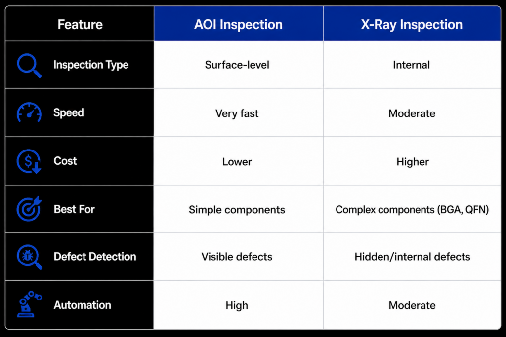
AOI vs X-Ray Inspection for PCB Assembly: A Side-by-Side Comparison
When evaluating AOI vs X-Ray inspection for PCB assembly, it’s important to understand that each technology serves a different purpose.
| Inspection Factor | AOI | X-Ray |
| Visible Defect Detection | Excellent | Good |
| Hidden Joint Inspection | Limited | Excellent |
| BGA Analysis | Limited | Excellent |
| Inspection Speed | Fast | Moderate |
| Equipment Cost | Lower | Higher |
| Production Volume Suitability | Excellent | Moderate |
| Internal Structure Visibility | No | Yes |
For standard SMT assemblies, AOI may provide sufficient coverage. For complex boards with hidden solder joints, X-Ray becomes increasingly valuable.
Which Inspection Method Meets IPC Standards Better?
Many manufacturers assume one technology is superior to the other, but IPC standards do not specifically mandate a single inspection method.
Instead, IPC focuses on whether the final product meets established quality requirements.
Where AOI Supports IPC Compliance?
AOI helps manufacturers verify:
- Component placement accuracy
- Solder quality
- Polarity correctness
- Visible assembly defects
This makes AOI an important tool in IPC standards PCB inspection programs.
Where X-Ray Supports IPC Compliance?
X-Ray inspection helps verify:
- Hidden solder joints
- BGA connections
- Internal solder voids
- Advanced package integrity
As electronics become more compact, these capabilities play an increasingly important role in compliance verification.
The Real Answer:
When comparing AOI vs X-Ray Inspection, the better solution often depends on the complexity of the assembly.
For simple boards, AOI may be sufficient.
For assemblies with BGAs, QFNs, or hidden solder joints, X-Ray often provides the deeper level of inspection needed to ensure quality and reliability.
Why Leading Manufacturers Use Both AOI and X-Ray?
Many of the most successful electronics manufacturers combine both technologies to maximize defect detection.
Using both inspection methods provides:
Greater Inspection Coverage:
Visible and hidden defects can be identified throughout the assembly process.
Improved Product Reliability:
Research from industry reliability studies shows that early defect detection significantly reduces field failures and warranty costs.
Reduced Rework Expenses:
Finding defects before products leave the facility is substantially less expensive than correcting failures after shipment.
Stronger Customer Confidence:
Customers gain assurance that products have undergone comprehensive inspection procedures.
This is why many advanced PCB manufacturing inspection services integrate AOI and X-Ray into their quality control workflow.
Choosing the Right Inspection Strategy:
The best inspection strategy depends on several factors:
- PCB complexity
- Component types
- Production volume
- Reliability requirements
- Customer specifications
For standard assemblies, AOI may offer excellent value and efficiency. For mission-critical electronics in aerospace, medical, automotive, and industrial applications, X-Ray often becomes essential.
Many providers of professional PCB manufacturing inspection services recommend a hybrid approach to achieve maximum quality assurance.
Partner With a Manufacturer That Prioritizes Quality:
Inspection technology plays a crucial role in product reliability, but equipment alone isn’t enough. Effective quality control requires experienced engineers, validated processes, and strict adherence to industry standards.
At Cygnus Electronics, quality is built into every stage of the manufacturing process. Our comprehensive inspection capabilities, advanced manufacturing practices, and commitment to IPC compliance help ensure every PCB assembly meets the highest standards of performance and reliability.
Whether your project requires AOI, X-Ray inspection, or a complete quality assurance strategy, Cygnus Electronics delivers the expertise and precision needed to support your success.
Contact Cygnus Electronics today to learn how our advanced PCB manufacturing and inspection solutions can help improve product quality, reduce defects, and accelerate production confidence.
Frequently Asked Questions
Is AOI enough for IPC compliance?
AOI can support IPC compliance for many PCB assemblies, especially when defects are visible. However, complex boards with hidden solder joints may require X-Ray inspection for complete verification.
Why is X-Ray inspection important for BGA components?
BGA solder joints are located underneath the component package and cannot be visually inspected. X-Ray allows manufacturers to evaluate these hidden connections without damaging the assembly.
Do IPC standards require X-Ray inspection?
No. IPC standards generally define quality and acceptability requirements rather than mandating specific inspection technologies.
Should manufacturers use both AOI and X-Ray inspection?
In many cases, yes. Combining AOI and X-Ray provides broader defect detection coverage and supports more comprehensive quality assurance programs.
The post AOI vs X-Ray Inspection: Which Meets IPC Standards Better? appeared first on Cygnus.
]]>The post Types of Flux in PCB Assembly: No-Clean vs Water-Soluble vs Rosin appeared first on Cygnus.
]]>Without the right flux, solder joints can fail, components may not bond properly, and long-term PCB reliability can suffer. From consumer electronics to aerospace systems, choosing the correct flux directly impacts manufacturing quality and product performance.
In this guide, we’ll break down the main types of flux in PCB assembly, compare no-clean flux vs water-soluble flux, explain the role of rosin flux in PCB assembly, and help manufacturers understand which option works best for different applications.
What Is Flux in PCB Assembly?
Flux is a chemical cleaning agent used during soldering to remove oxidation, improve solder flow, and help create strong electrical connections between components and the PCB.
During soldering, metal surfaces naturally develop oxidation when exposed to air. This oxidation prevents solder from bonding correctly. Flux removes these contaminants and improves solder adhesion.
The main functions of flux include:
- Removing oxides from metal surfaces
- Improving solder wetting
- Preventing re-oxidation during heating
- Enhancing solder joint reliability
- Reducing soldering defects
In simple terms, flux helps solder “stick” properly.
Without proper flux, manufacturers may experience:
- Cold solder joints
- Poor conductivity
- Solder bridging
- Weak mechanical bonds
- Corrosion-related failures
This is why selecting the right PCB soldering flux types is critical in electronics manufacturing.
Why Flux Matters More in Modern PCB Assembly?
Today’s PCBs are far more advanced than older electronic boards. Manufacturers now deal with:
- Miniaturized SMT components
- Fine-pitch packages
- High-density PCB layouts
- Lead-free soldering temperatures
- Faster automated production lines
These factors make flux performance even more important.
According to IPC industry studies, soldering defects account for a significant percentage of PCB manufacturing failures, with poor wetting and contamination among the leading causes in assembly defects.
As PCB complexity increases, manufacturers need better:
- Solder wetting improvement
- Residue control
- Thermal stability
- Cleaning compatibility
- Reliability under harsh conditions
This is where understanding the differences between flux types becomes essential.
Main Types of Flux in PCB Assembly:
There are three major types of flux in PCB assembly commonly used in electronics manufacturing:
- No-Clean Flux
- Water-Soluble Flux
- Rosin Flux
Each type offers different advantages depending on the application, cleaning requirements, reliability standards, and production environment.
No-Clean Flux Explained
What Is No-Clean Flux?
No-clean flux is designed to leave minimal residue after soldering, reducing or eliminating the need for post-solder cleaning.
It is one of the most widely used PCB soldering flux types in high-volume electronics manufacturing because it simplifies production and lowers operational costs.
Advantages of No-Clean Flux:
Faster Manufacturing:
Since cleaning is often unnecessary, production moves faster.
Lower Operational Costs:
Manufacturers save on:
- Cleaning chemicals
- Water usage
- Cleaning equipment
- Labor costs
Better for High-Volume SMT Assembly:
No-clean flux works especially well in automated SMT production environments.
Environmentally Friendlier
Reduced chemical cleaning means lower environmental impact.
Challenges of No-Clean Flux:
While efficient, no-clean flux does have limitations.
Flux Residue in PCB Assembly:
Even minimal residue can sometimes:
- Affect conformal coating adhesion
- Complicate inspection
- Cause reliability concerns in sensitive applications
Difficult Rework:
Residue may become difficult to remove during PCB repairs.
Not Ideal for Harsh Environments:
Industries like aerospace and medical electronics may require cleaner assemblies with stricter reliability standards.
Water-Soluble Flux Explained:
What Is Water-Soluble Flux?
Water-soluble flux contains organic compounds designed for aggressive oxide removal and excellent solderability.
Unlike no-clean flux, it requires a full PCB cleaning process after soldering.
Advantages of Water-Soluble Flux:
Excellent Solder Wetting Improvement:
Water-soluble flux provides outstanding solder flow and bonding performance.
This makes it ideal for:
- Complex SMT assemblies
- Fine-pitch components
- High-density PCBs
Better Oxide Removal:
It performs well on heavily oxidized surfaces.
Superior Reliability:
When cleaned correctly, it leaves very little contamination behind.
Challenges of Water-Soluble Flux:
Mandatory Cleaning Process:
Improper cleaning can leave ionic contamination behind, increasing corrosion risks.
Higher Manufacturing Costs:
Manufacturers must invest in:
- Cleaning systems
- DI water systems
- Drying equipment
- Process monitoring
Moisture Sensitivity:
Residual contamination can absorb moisture and impact PCB reliability.
Rosin Flux in PCB Assembly:
What Is Rosin Flux?
Rosin flux in PCB assembly is made from natural pine resin and has been used in electronics manufacturing for decades.
It remains popular in specialized applications because of its strong oxidation protection and reliable soldering performance.
Types of Rosin Flux:
R (Rosin):
Mild activation level with low cleaning power.
RMA (Rosin Mildly Activated):
Balanced cleaning ability and residue characteristics.
RA (Rosin Activated):
Highly aggressive cleaning action for difficult surfaces.
Advantages of Rosin Flux:
Reliable Soldering Performance:
Rosin flux performs consistently across many soldering applications.
Good Oxidation Protection:
It helps protect metal surfaces during soldering.
Proven Industry History:
Many military and industrial applications still use rosin-based formulations.
Challenges of Rosin Flux:
Residue Removal:
Rosin residue often requires solvent cleaning.
Smoke and Fumes:
Rosin fumes may require proper ventilation systems.
Environmental Concerns:
Traditional solvent cleaning methods may not align with modern environmental standards.
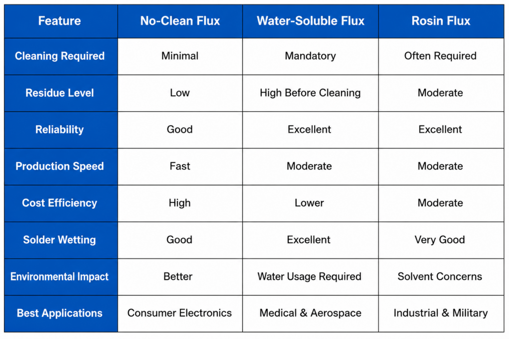
No-Clean Flux vs Water-Soluble Flux vs Rosin Flux:
Here’s a practical comparison of the most common PCB soldering flux types:
Lead-Free Soldering Flux Challenges:
The transition toward lead-free soldering flux systems has introduced new manufacturing challenges.
Lead-free solder alloys melt at higher temperatures compared to traditional tin-lead solder. This increases:
- Thermal stress
- Oxidation risk
- Flux activation demands
As a result, manufacturers now require fluxes with:
- Better thermal stability
- Stronger oxide removal
- Improved residue control
According to electronics manufacturing industry reports, lead-free soldering can increase soldering temperatures by 30–40°C compared to traditional processes.
This makes flux chemistry more important than ever.
The Importance of Flux Residue Control:
One of the biggest concerns in modern assembly is flux residue in PCB assembly.
Improper residue management can cause:
- Corrosion
- Dendritic growth
- Electrical leakage
- Signal interference
- Reduced product lifespan
This is especially critical in:
- Medical devices
- Automotive electronics
- Aerospace systems
- High-frequency PCBs
Manufacturers often perform:
- Ionic contamination testing
- Visual inspection
- SIR testing (Surface Insulation Resistance)
- Cleanliness verification
to ensure long-term PCB reliability.
How to Choose the Right Flux?
There is no universal “best” flux.
The right choice depends on:
- PCB complexity
- Reliability requirements
- Production volume
- Cleaning capabilities
- Environmental conditions
- Industry standards
Choose No-Clean Flux If:
- You need faster production
- Cost efficiency matters
- Minimal cleaning is preferred
Choose Water-Soluble Flux If:
- Reliability is critical
- You can support full cleaning systems
- Your application requires ultra-clean assemblies
Choose Rosin Flux If:
- You need strong oxidation protection
- You work in specialized industrial applications
- Traditional processes are preferred
Flux Selection Trends in Electronics Manufacturing:
Modern PCB manufacturing is shifting toward:
- Low-residue formulations
- Eco-friendly chemistries
- Better lead-free compatibility
- Automated flux control systems
Manufacturers are increasingly focusing on:
- Process consistency
- Lower defect rates
- Sustainability
- High-reliability assembly standards
This evolution continues to drive innovation in lead-free soldering flux technologies and automated cleaning systems.
Final Thoughts:
Choosing between no-clean flux vs water-soluble flux or deciding whether rosin flux in PCB assembly is suitable for your application can significantly impact manufacturing quality, production efficiency, and long-term reliability.
The best flux is not simply the cheapest or fastest option. It’s the one that aligns with your:
- PCB design
- Reliability goals
- Production process
- Industry requirements
As electronics continue becoming more advanced, flux chemistry remains one of the most important foundations of reliable PCB assembly.
Need Reliable PCB Assembly Support?
Cygnus Electronics provides professional PCB assembly and electronics manufacturing solutions with a strong focus on quality, process control, SMT/THT assembly, inspection, and reliable production practices. Whether you need prototype builds or scalable manufacturing support, their team helps ensure dependable electronics manufacturing outcomes.
The post Types of Flux in PCB Assembly: No-Clean vs Water-Soluble vs Rosin appeared first on Cygnus.
]]>The post IPC Standards for Solder Joint Quality Explained Simply appeared first on Cygnus.
]]>That’s where IPC standards for solder joints come in. Not to complicate things but to make sure your electronics actually work when they leave the factory.
Let’s break it down without turning it into a technical headache.
What Are IPC Standards?
IPC standards are globally accepted guidelines that define how electronic products should be designed, assembled, and inspected.
Think of them as the rulebook for electronics manufacturing:
- What a good solder joint looks like
- What counts as a defect
- What level of quality is acceptable
Without these standards, “quality” becomes subjective and that’s never a good idea in production.
Why IPC Standards Matter for Solder Joint Quality?
Ignoring standards might save time upfront. It almost always costs more later.
Here’s why they matter:
Consistency Across Production:
Every unit follows the same quality benchmark.
Reduced Defects and Rework:
Clear criteria mean fewer mistakes slipping through.
Improved Product Reliability:
Strong solder joints = longer-lasting electronics.
Industry Compliance:
Many industries require strict adherence to IPC soldering standards.
Key IPC Standards for Solder Joints:
Not all standards are created equal. These are the ones that actually matter:
IPC-A-610:
Focuses on the acceptability of electronic assemblies. It visually defines what’s acceptable and what’s not.
IPC-J-STD-001:
Covers the requirements for soldered electrical assemblies.This is more process-focused on how soldering should be done.
IPC-7711/7721:
Deals with rework and repair standards. Because let’s be honest, mistakes happen.
If you’re serious about solder joint quality standards, these are non-negotiable.
IPC Solder Joint Classifications (Class 1, 2, 3):
Not every product needs the same level of perfection.
Class 1 – General Electronics:
Basic consumer products where performance isn’t critical.
Class 2 – Dedicated Service Electronics:
Products that need reliability but aren’t life-critical.
Class 3 – High-Reliability Electronics:
Medical, aerospace, and critical systems. Failure is not an option.
Choosing the wrong class can either increase costs unnecessarily or worse, reduce reliability.
Also Read: Impact of Incorrect Flux Volume on Soldering Quality and Reliability
What Makes a Good Solder Joint According to IPC?
A proper solder joint isn’t about looking “okay.” It has specific characteristics:
- Smooth and shiny appearance
- Proper wetting on both pad and lead
- Well-formed fillet
- No cracks, voids, or gaps
If your joints don’t meet these basics, they’re already a risk.
Also Read: What Does Flux Do in Soldering? (Complete Guide)
Common Soldering Defects Identified by IPC:
Even with standards, defects still happen. The difference is you can catch them early.
Cold Solder Joints:
Weak connections due to improper heating.
Solder Bridging:
Unwanted connections between pads.
Insufficient Solder:
Not enough material to form a strong bond.
Voiding:
Air pockets that weaken the joint.
These are the same issues that quietly explain why solder joints fail in electronics.
How to Meet IPC Standards in PCB Assembly?
Meeting standards isn’t about memorizing rules. It’s about controlling your process.
Train and Certify Your Team:
Skilled operators make a huge difference.
Maintain Equipment:
Inconsistent machines = inconsistent results.
Use Quality Materials:
Cheap inputs lead to poor outputs. Always.
Implement Proper Inspection
AOI, X-ray, and testing ensure compliance.
Following IPC standards for solder joints isn’t optional if you care about quality—it’s essential.
Final Thoughts:
IPC standards aren’t there to slow you down. They’re there to protect your product, your reputation, and your bottom line. Because in electronics manufacturing, small defects don’t stay small for long.
FAQs
What are IPC standards in electronics?
IPC standards are global guidelines that define quality, reliability, and manufacturing processes for electronic products.
Which IPC standard is used for solder joint quality?
IPC-A-610 and IPC-J-STD-001 are the most widely used standards for solder joint quality and assembly requirements.
What are IPC Class 1, 2, and 3 products?
They represent reliability levels—Class 1 for basic products, Class 2 for reliable electronics, and Class 3 for critical applications.
How do IPC standards improve PCB quality?
They provide clear acceptance criteria, reduce defects, and ensure consistent manufacturing quality across production.
The post IPC Standards for Solder Joint Quality Explained Simply appeared first on Cygnus.
]]>The post AOI vs X-Ray Inspection in SMT appeared first on Cygnus.
]]>That’s why choosing the right SMT inspection methods isn’t optional anymore, it’s critical.
If you’re deciding between AOI vs X-ray inspection in SMT, this guide will break it down clearly, practically, and from a real manufacturing perspective so you can make the right call.
What Is AOI and X-Ray Inspection in SMT?
AOI (Automated Optical Inspection) uses high-resolution cameras to visually inspect the PCB surface for defects like misalignment, missing components, or solder bridging.
X-ray inspection PCB systems, on the other hand, look inside the board detecting hidden defects in solder joints, especially in complex packages like BGAs.
In simple terms:
- AOI = What you can see
- X-ray = What you can’t see
Why PCB Inspection Matters in SMT Assembly?
Here’s the reality: most PCB failures don’t happen in design, they happen in manufacturing.
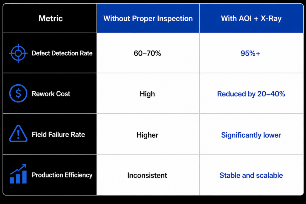
- Up to 70% of electronic failures are linked to solder joint issues
- Rework can increase production costs by 15–30%
- Field failures damage brand trust and increase warranty claims
A strong PCB quality inspection process ensures:
- Early defect detection
- Lower rework costs
- Higher product reliability
How AOI Inspection Works in SMT?
AOI inspection PCB systems operate as your first line of defense in the production line.
Step-by-Step AOI Process:
- High-speed cameras capture PCB images
- Software compares images with reference data (Gerber files)
- AI/algorithms detect inconsistencies
- Defects are flagged for review
What AOI Can Detect:
- Missing components
- Misaligned parts
- Polarity errors
- Solder bridges
- Excess or insufficient solder
AOI is fast, scalable, and ideal for high-volume production.
How X-Ray Inspection Works in PCB Assembly?
When defects hide beneath components, X-ray inspection PCB becomes essential.
How It Works:
- X-rays penetrate PCB layers
- Internal structures are visualized
- Software analyzes solder joints and connections
What X-Ray Inspection Detects:
- Voids in solder joints
- Cracks and internal fractures
- Hidden bridges
- Insufficient solder under components
This is especially critical for:
BGA inspection methods:
- QFN packages
- Multilayer boards
If your product uses advanced components, X-ray inspection solder joints is non-negotiable.
AOI vs X-Ray Inspection in SMT: Key Differences
This comparison makes one thing clear: Both methods solve different problems.
Advantages of AOI in SMT Manufacturing:
Why do most manufacturers rely heavily on AOI?
- Fast inline inspection
- Cost-effective for mass production
- Detects common assembly defects
- Easy integration into production lines
For basic PCB inspection techniques, AOI is the backbone.
Advantages of X-Ray Inspection in PCB Assembly:
When precision matters, X-ray delivers.
- Detects hidden defects
- Essential for BGA inspection
- High accuracy in solder joint evaluation
- Reduces field failure risks
For critical applications, X-ray inspection PCB is a game-changer.
Limitations of AOI vs X-Ray Inspection:
AOI Limitations:
- Cannot detect hidden solder joints
- May produce false positives
- Limited for complex assemblies
X-Ray Limitations:
- Higher equipment cost
- Slower compared to AOI
- Requires skilled operators
Knowing limitations helps you build a smarter inspection strategy.
When Should You Use AOI vs X-Ray in SMT?
Here’s a practical breakdown:
- Use AOI when:
- High-volume production
- Standard components
- Need fast inspection
- Use X-ray when:
- Complex PCB designs
- BGA/QFN components
- High reliability required
Best practice? Use both together.
Also Read: How Surface Mount Technology Increases PCB Assembly Efficiency?
AOI + X-Ray: The Smart Inspection Strategy
Relying on one method alone leaves gaps.
Combining both ensures:
- Surface + internal inspection
- Reduced defect escape rate
- Improved product reliability
- Higher production yield
This is how modern manufacturers optimize their PCB quality inspection process.
Real Impact of Inspection Methods (Industry Stats)
The takeaway: Better inspection = better margins + better products
How to Choose the Right PCB Inspection Technique
Before choosing between SMT inspection methods, consider:
- PCB complexity
- Component type (BGA, QFN, etc.)
- Production volume
- Budget
- Reliability requirements
There’s no one-size-fits-all only the right combination.
Build Reliable Electronics with the Right Inspection Partner
Choosing the right inspection method is important. But choosing the right manufacturing partner? That’s what truly defines your product quality.
At Cygnus Electronics, advanced PCB inspection techniques are built into every stage of production from AOI inspection PCB systems to high-precision X-ray inspection solder joints analysis.
If you want fewer defects, faster production, and reliable electronics:
Work with Cygnus and build it right the first time.
Final Takeaway:
If you’re still thinking about AOI vs X-ray inspection in SMT, you’re asking the wrong question.
The real answer is: Use both and build a complete inspection strategy.
Because in electronics manufacturing, what you don’t see…
is exactly what causes failures later.
FAQs
What is the difference between AOI and X-ray inspection in SMT?
AOI detects visible surface defects using cameras, while X-ray inspection identifies hidden defects inside solder joints and components.
Is AOI enough for PCB inspection?
AOI is effective for surface-level inspection but cannot detect internal defects. For complex PCBs, combining AOI with X-ray inspection is recommended.
Why is X-ray inspection important for BGA components?
BGA components have hidden solder joints that cannot be visually inspected. X-ray inspection ensures these joints are properly formed and reliable.
Which inspection method is more accurate?
X-ray inspection is more accurate for internal defects, while AOI is faster and efficient for surface-level inspection. Both are complementary.
The post AOI vs X-Ray Inspection in SMT appeared first on Cygnus.
]]>The post Cold Solder Joints in Reflow: Hidden Risks You Shouldn’t Ignore appeared first on Cygnus.
]]>That’s the danger of cold solder joints in reflow soldering: they don’t always show obvious signs at first. Yet over time, they quietly weaken connections, leading to intermittent failures, costly repairs, and even product recalls.
If you’re working with PCB assembly, understanding and preventing these defects isn’t optional, it’s essential for long-term reliability.
What Is a Cold Solder Joint in Reflow Soldering?
A cold solder joint occurs when the solder does not fully melt or properly bond during the reflow process, resulting in a weak electrical and mechanical connection. These joints often appear dull or uneven and can cause unstable circuit performance or complete failure over time.
In simple terms, it’s a connection that looks done but isn’t truly reliable.
How to Identify a Cold Solder Joint?
Spotting a cold solder joint PCB issue early can save significant time and cost. Here are the most common cold solder joint symptoms:
- Dull, grainy, or matte surface instead of a shiny finish
- Visible cracks or uneven solder distribution
- Poor wetting between component leads and pads
- Intermittent or unstable electrical signals
These are also considered key signs of bad solder joints, especially in high-density PCB assemblies.
 Advanced detection methods include:
- Automated Optical Inspection (AOI)
- X-ray inspection (for hidden joints)
- Functional circuit testing
Why Cold Solder Joints Occur in Reflow Soldering?
Understanding the cold solder joint causes helps you prevent them at the source. Here are the most common reasons:
Insufficient Reflow Temperature:
If the temperature doesn’t reach the required level, solder won’t fully melt—resulting in weak bonding.
Improper Temperature Profile:
Incorrect soak time or uneven heating can prevent proper solder flow across the joint.
Poor Solder Paste Quality:
Expired or contaminated solder paste affects melting behavior and adhesion.
Oxidation on PCB or Components:
Oxidized surfaces block proper solder wetting, leading to weak joints.
Inadequate Flux Activity:
Flux plays a critical role in cleaning surfaces. If it’s ineffective, bonding fails.
These cold solder joint causes are often interconnected, making process control critical.
Hidden Risks of Cold Solder Joints:
Here’s where things get serious.
Cold solder joints in reflow soldering don’t just affect appearance they directly impact performance and reliability.
 Key Risks:
- Intermittent circuit failures (hard to diagnose)
- Reduced product lifespan
- Increased warranty claims and returns
- Field failures in critical applications
- Safety risks in automotive, medical, or industrial systems
 Industry insight:
A significant percentage of reflow soldering defects are linked to poor joint formation, making this a major reliability concern.
If you care about solder joint reliability PCB, this is a defect you cannot ignore.
Cold Solder Joints vs Proper Solder Joints:
| Feature | Cold Solder Joint | Proper Solder Joint |
| Appearance | Dull, rough | Smooth, shiny |
| Mechanical Strength | Weak | Strong |
| Electrical Conductivity | Unstable | Reliable |
| Long-Term Reliability | Poor | High |
How to Prevent Cold Solder Joints in Reflow?
Prevention is always more cost-effective than rework. Here’s how to improve solder joint reliability PCB:
Optimize Reflow Temperature Profile:
Ensure proper preheat, soak, peak, and cooling phases.
Use High-Quality Solder Paste:
Store paste correctly and avoid expired materials.
Maintain Clean PCB Surfaces:
Remove oxidation and contamination before assembly.
Ensure Accurate Stencil Printing:
Consistent solder paste deposition is critical.
Use the Right Flux Chemistry:
Match flux type with your process and materials.
These steps significantly reduce reflow soldering defects and improve overall production quality.
Inspection & Testing Methods:
To detect issues in a cold solder joint PCB, use:
- AOI (Automated Optical Inspection) – for visible defects
- X-ray Inspection – for hidden joints like BGAs
- Functional Testing – to verify real-world performance
- Thermal Stress Testing – to test durability under load
Early detection helps avoid major downstream failures.
Why the Right EMS Partner Makes All the Difference?
Cold solder joints are not just a technical issue they’re a process issue.
That’s why working with an experienced EMS provider matters.
With Cygnus Electronics, you get:
- Optimized reflow profiles
- Advanced inspection (AOI, X-ray)
- Strict quality control processes
- End-to-end PCB assembly expertise
Don’t let hidden defects compromise your product.
Partner with experts who prioritize precision and reliability from design to production.
Conclusion:
Cold solder joints may seem minor but their impact is anything but.
From hidden failures to costly recalls, these defects can quietly damage your product’s reputation and performance.
By understanding cold solder joint symptoms, addressing signs of bad solder joints, and eliminating root causes, you can build more reliable, high-performing PCBs.
In manufacturing, it’s not just about making connections it’s about making reliable connections that last.
FAQs
What causes cold solder joints in reflow soldering?
Cold solder joints are caused by insufficient heat, poor temperature profiles, oxidation, or low-quality solder paste that prevents proper bonding.
How can you identify cold solder joint symptoms?
Common cold solder joint symptoms include dull appearance, cracks, uneven solder, and unstable electrical performance.
Why are cold solder joints dangerous?
They lead to intermittent failures, reduced reliability, and long-term product issues, especially in critical applications.
What are the signs of bad solder joints?
Typical signs of bad solder joints include poor wetting, grainy texture, weak bonding, and inconsistent electrical conductivity.
The post Cold Solder Joints in Reflow: Hidden Risks You Shouldn’t Ignore appeared first on Cygnus.
]]>The post How Solder Paste Quality Impacts Reflow Defects (Complete Guide) appeared first on Cygnus.
]]>But in reality…
It’s one of the biggest factors behind whether your PCB works perfectly or fails in the field.
A slight inconsistency in solder paste quality can trigger a chain reaction: poor wetting, uneven heating, and ultimately, costly reflow soldering defects.
And here’s the part most manufacturers overlook: Many of the causes of soldering defects don’t start in the oven they start at the paste stage.
In this guide, we’ll break down how solder paste in PCB assembly influences defect formation, what goes wrong, and most importantly how to prevent reflow defects before they even begin.
What Is Solder Paste in PCB Assembly?
Solder paste in PCB assembly is a mixture of microscopic solder alloy particles and flux. It is applied to the PCB pads before components are placed and soldered during the reflow process.
Key Components:
- Solder Alloy (e.g., SAC305): Forms the electrical and mechanical bond
- Flux: Removes oxides and enables proper wetting
- Additives: Control viscosity and performance
Why It Matters:
The performance of solder paste in PCB assembly determines:
- How well components adhere
- How evenly solder melts
- How reliable the final connection is
Why Solder Paste Quality Matters in Reflow Soldering?
Think of solder paste as the foundation of your PCB.
If the foundation is unstable, everything built on top of it is at risk.
Impact on Solder Joint Reliability:
Poor solder paste quality leads to weak bonds, directly affecting solder joint reliability PCB performance.
Influence on Manufacturing Yield:
Defective paste increases rejection rates, rework, and production delays.
Increased Defect Rates:
Studies show a significant portion of reflow soldering defects are linked to paste-related issues.
This is why solder paste quality is not just a material choice it’s a production strategy.
Common Reflow Defects Caused by Poor Solder Paste Quality:
When solder paste defects occur, they often show up as visible and performance issues during reflow.
Solder Bridging:
- Excess paste causes connections between adjacent pads
Tombstoning:
- Uneven wetting lifts one side of a component
Voiding:
- Trapped gases from poor flux lead to air pockets
Solder Balling:
- Paste splatter due to contamination or poor formulation
Cold Solder Joints:
- Improper flux activation prevents proper bonding
These are some of the most common causes of soldering defects, and most of them trace back to paste issues not just temperature profiles.
Key Factors That Define Solder Paste Quality:
Not all paste is created equal.
Here’s what separates high-performance paste from problematic ones:
Particle Size & Distribution:
- Fine pitch boards require smaller particles (Type 4 or 5)
Flux Chemistry:
- Determines wetting and oxide removal efficiency
Viscosity & Rheology:
- Controls how paste spreads and holds shape
Shelf Life & Storage:
- Degraded paste leads to inconsistent printing
Oxidation Levels:
- Oxidized particles reduce bonding strength
Each of these directly impacts the solder paste impact on reflow and overall process stability.
Also Read: Common Reflow Soldering Defects
How Solder Paste Quality Affects the Reflow Process?
The solder paste impact on reflow is seen across multiple stages:
Printing Performance:
- Poor paste → uneven deposits
Wetting Behavior:
- Low-quality paste → incomplete bonding
Slump Control:
- Excess spreading → bridging defects
Outgassing:
- Poor flux → increased voiding
This is where solder paste quality becomes critical—not just before reflow, but throughout the entire thermal cycle.
Signs of Poor Solder Paste Quality (Quick Diagnosis):
Not sure if your paste is the issue?
Watch for these signs:
- Inconsistent paste deposits
- Excessive solder balls
- Poor wetting and bonding
- High defect rates during inspection
These indicators often point directly to solder paste defects rather than process issues.
Best Practices to Maintain Solder Paste Quality:
If you want to improve solder joint reliability PCB performance, start here:
roper Storage:
- Keep paste at controlled temperatures (0–10°C)
Controlled Thawing:
- Avoid condensation and moisture issues
Stencil Maintenance:
- Clean regularly to ensure consistent printing
Paste Handling:
- Mix properly before use
FIFO Method:
- Use older paste first to avoid degradation
These steps are essential when learning how to prevent reflow defects effectively.
Also Read: Impact of Incorrect Flux Volume on Soldering Quality and Reliability
How to Choose the Right Solder Paste?
Choosing the right paste depends on:
PCB Complexity:
- High-density boards require finer paste
Component Size:
- Fine pitch → smaller particle size
Thermal Profile:
- Match paste with reflow conditions
Industry Requirements:
- Automotive & medical need higher reliability
The right selection improves both performance and reduces the risk of reflow soldering defects.
Advanced Insight: How Experts Optimize Solder Paste Performance
Modern EMS providers don’t rely on guesswork.
They use:
- Process monitoring systems
- AOI & X-ray inspection
- Data-driven optimization
This ensures maximum solder joint reliability PCB and minimal defect rates.
Conclusion:
In PCB manufacturing, small details create big outcomes.
And solder paste quality is one of those details that quietly determines success or failure.
From preventing solder paste defects to improving yield and reliability, the right approach to paste selection and handling can transform your entire production process.
If you want to consistently reduce defects and improve performance, the focus shouldn’t just be on reflow profiles…
…it should start with the paste itself.
FAQs
What defects are caused by poor solder paste quality?
Poor solder paste quality can cause bridging, tombstoning, voiding, solder balling, and cold joints due to improper wetting and contamination.
How does solder paste affect reflow soldering?
Solder paste in PCB assembly controls how components bond during reflow, directly influencing wetting, heat transfer, and defect formation.
What are the main causes of soldering defects?
The most common causes of soldering defects include poor paste quality, incorrect storage, improper stencil design, and incorrect reflow profiles.
How can you prevent reflow defects?
To prevent reflow defects, ensure proper paste storage, correct handling, optimized stencil design, and controlled reflow profiles.
The post How Solder Paste Quality Impacts Reflow Defects (Complete Guide) appeared first on Cygnus.
]]>The post PCB Pad Design Guidelines to Avoid Reflow Issues appeared first on Cygnus.
]]>That’s why understanding PCB pad design guidelines isn’t optional, it’s essential. If you want fewer defects, better yields, and reliable boards, it all begins here.
What Is PCB Pad Design?
PCB pad design refers to the layout, size, and shape of conductive areas on a PCB where components are soldered.
These pads act as the connection point between components and the board. In PCB pad design for reflow soldering, even minor inconsistencies can affect how solder melts, flows, and solidifies.
Why PCB Pad Design Matters in Reflow Soldering?
Pad design directly controls solder behavior during reflow.
If your pad design is off, you’re likely to face:
- Uneven solder distribution
- Component misalignment
- Weak solder joints
Good PCB pad design to avoid soldering defects ensures:
- Balanced heat distribution
- Stable component placement
- Consistent solder joints
In short, it’s one of the most effective strategies for reflow soldering defects prevention.
Common Reflow Issues Caused by Poor Pad Design:
Before fixing the problem, it’s important to recognize it.
1. Tombstoning:
One side of a component lifts during reflow due to uneven heating or pad imbalance.
2. Solder Bridging:
Excess solder or tight spacing causes unintended connections between pads.
3. Solder Balling:
Small solder spheres form due to improper solder paste control or pad design.
4. Insufficient or Excess Solder:
Leads to weak joints or short circuits.
Most of these issues trace back to poor pad geometry or layout decisions.
Key PCB Pad Design Guidelines to Avoid Reflow Issues:
This is where real improvement happens. Follow these SMT pad design best practices to ensure better results.
1. Optimize Pad Size and Shape:
- Match pad dimensions to component specifications
- Avoid oversized pads (can cause solder bridging)
- Avoid undersized pads (leads to weak joints)
Proper sizing improves solder joint reliability PCB performance.
2. Maintain Proper Pad Spacing:
- Ensure adequate clearance between pads
- Follow IPC standards for spacing
- Prevent solder bridging during reflow
Spacing isn’t just design it’s defect prevention.
3. Ensure Thermal Balance:
- Keep pad sizes symmetrical
- Avoid uneven copper distribution
- Ensure equal heat exposure
Uneven heating is a major cause of tombstoning.
4. Control Solder Paste Volume:
- Use precise solder paste stencil design
- Avoid excessive solder deposition
- Ensure uniform paste distribution
Too much solder = bridging
Too little solder = weak joints
Balance is everything.
5. Maintain Pad Symmetry:
- Symmetrical pad design keeps components stable
- Reduces shifting during reflow
- Improves placement accuracy
6. Choose the Right Solder Mask Design:
- NSMD (Non-Solder Mask Defined): Better solder joint reliability
- SMD (Solder Mask Defined): Better for fine-pitch components
Choosing the right type impacts long-term durability.
IPC Standards and Best Practices for Pad Design:
Following industry standards isn’t just a recommendation it’s a necessity.
Key Standard: IPC-7351
- Defines pad dimensions and layouts
- Ensures compatibility with components
- Reduces manufacturing risks
Aligning your design with IPC standards strengthens PCB layout design tips and improves production consistency.
Also Read: Reworking and Repairing Coated PCBs: What You Need to Know?
How Pad Design Impacts Solder Joint Reliability?
The strength of your PCB depends on the quality of its solder joints.
Good pad design ensures:
- Strong mechanical bonding
- Reliable electrical connections
- Resistance to thermal stress
Poor design, on the other hand, leads to:
- Cracked joints
- Intermittent connections
- Reduced product lifespan
This is why solder joint reliability PCB performance starts at the design stage—not during assembly.
Design for Manufacturability (DFM) in PCB Pad Layout:
Great designs don’t just look good they manufacture well.
Why DFM matters:
- Identifies design issues before production
- Reduces costly rework
- Improves yield and efficiency
Collaborating with manufacturers early ensures your PCB pad design for reflow soldering is optimized from day one.
Tools and Software for Optimizing PCB Pad Design:
Modern tools make it easier to avoid errors.
Popular tools:
- Altium Designer
- KiCad
- Eagle PCB
What they help with:
- Design rule checks (DRC)
- Thermal simulation
- Pad and footprint optimization
Using the right tools strengthens your PCB layout design tips and minimizes risks.
How EMS Providers Improve PCB Pad Design in Canada?
Working with experienced EMS partners can significantly reduce defects.
They offer:
- Design validation and DFM reviews
- Prototyping and testing
- Process optimization for reflow
This is especially valuable for complex or high-volume production.
Improve Your PCB Reliability with Expert Support:
If you want to reduce defects, improve yield, and ensure long-term performance, the right partner makes all the difference.
Cygnus Electronics provides expert PCB assembly support, including design validation, process optimization, and advanced manufacturing solutions. Their team helps you implement proven PCB pad design guidelines and SMT pad design best practices—so your boards perform reliably from prototype to production.
Final Thoughts: Design Smarter, Manufacture Better
Reflow defects aren’t random they’re predictable. And more importantly, they’re preventable.
By following the right PCB pad design guidelines, optimizing solder paste stencil design, and focusing on manufacturability, you can eliminate common issues before they even begin.
Because in PCB manufacturing, the best fix… is designing it right the first time.
FAQs
What are PCB pad design guidelines?
They are best practices for pad size, spacing, and layout to ensure proper soldering and reliable PCB performance.
How does PCB pad design affect reflow soldering?
It controls solder flow, heat distribution, and component stability, directly impacting defect rates.
What is the role of solder paste stencil design?
It determines how much solder is applied to pads, affecting joint quality and preventing defects like bridging.
How can I improve solder joint reliability in PCB assembly?
By optimizing pad design, ensuring thermal balance, and following SMT pad design best practices.
The post PCB Pad Design Guidelines to Avoid Reflow Issues appeared first on Cygnus.
]]>The post How EMI Filtering Improves Signal Integrity in Electronics? appeared first on Cygnus.
]]>One of the biggest challenges engineers face is maintaining signal integrity in electronics. When signals become distorted or disrupted, devices may behave unpredictably, communication systems may fail, and sensitive components may stop functioning properly.
This is where EMI filtering in electronics becomes essential. By reducing unwanted electrical noise, EMI filters help circuits operate more reliably and ensure signals travel through systems accurately.
In this article, we’ll explore what EMI filtering in electronics is, why signal integrity matters, and how EMI filtering improves signal integrity in modern electronic systems.
What Is EMI Filtering?
Before understanding its benefits, it’s important to first define what EMI filtering in electronics means.
EMI stands for Electromagnetic Interference. It refers to unwanted electrical noise that disrupts signals within electronic circuits. This noise can come from many sources such as motors, switching power supplies, wireless devices, or even nearby electronic equipment.
EMI filtering in electronics is the process of suppressing or blocking this unwanted noise while allowing the intended signals to pass through the circuit.
This process, often referred to as electromagnetic interference filtering, uses specialized components such as capacitors, inductors, and ferrite beads to eliminate high-frequency noise that could otherwise disrupt circuit performance.
In simple terms, EMI filters act like a gatekeeper, allowing clean signals to pass while stopping electrical noise from entering or leaving a system.
What Is Signal Integrity and Why It Matters?
To understand why EMI filtering is important, we must first understand the concept of signal integrity in electronics.
Signal integrity refers to the quality, accuracy, and reliability of electrical signals as they travel through a circuit. When signals remain stable and undistorted, electronic systems perform as expected.
However, when signal integrity is compromised, several problems may occur, including:
- Data transmission errors
- Signal distortion
- Timing issues in digital systems
- Communication failures between components
Maintaining strong signal integrity in electronics is especially critical in modern systems where signals travel at extremely high speeds. Even small disturbances can lead to major performance issues.
This is why engineers place a strong focus on noise reduction and filtering when designing electronic circuits.
Also Read: How Power Line Filters Work (With Simple Explanation)
How Electromagnetic Interference Disrupts Electronic Signals?
Electronic circuits operate using electrical signals that carry information. When unwanted interference enters the system, it introduces noise that can alter these signals.
This interference can occur in two main forms:
Conducted EMI
Conducted interference travels through wires, cables, and power lines. It enters circuits through electrical connections and spreads through the system.
Radiated EMI
Radiated interference spreads through electromagnetic waves and can affect nearby circuits without direct electrical contact.
Sources of electromagnetic interference include:
- Power supplies
- Electric motors
- Wireless transmitters
- Switching electronics
- Industrial equipment
Without proper electromagnetic interference filtering, this noise can distort signals, causing inaccurate readings, communication errors, and unstable system performance.
How EMI Filtering Improves Signal Integrity in Electronics?
The primary purpose of EMI filters is to protect circuits from unwanted electrical noise. By doing so, they play a critical role in maintaining reliable signals.
So, how EMI filtering improves signal integrity can be understood through several key functions.
First, EMI filters block high-frequency noise from entering circuits through power lines or signal paths. This prevents interference from corrupting sensitive signals.
Second, EMI filters stabilize electrical signals by reducing fluctuations caused by electromagnetic noise. This helps signals remain clean and consistent.
Third, filtering prevents noise from spreading across different parts of a system. In complex electronics, interference in one component can easily affect others if not controlled.
Through EMI filtering in electronics, circuits can maintain accurate signal transmission, ensuring devices function properly even in noisy electrical environments.
Also Read: EMI Filter vs Surge Suppressor: Which One Protects Your Equipment Better?
Types of EMI Filters Used in Electronic Systems:
Engineers use different types of filters depending on where interference occurs and how signals travel through the system.
Power Line EMI Filters:
Power lines are one of the most common paths through which electrical noise enters electronic systems. Power line filters block unwanted noise coming from the electrical grid or nearby equipment.
These filters are widely used in industrial equipment, medical devices, and consumer electronics.
PCB EMI Filters:
Many modern devices integrate filtering components directly on the circuit board. These filters suppress interference at the source and help maintain signal integrity in electronics within the PCB itself.
Common Mode and Differential Mode Filters:
EMI can appear in different forms depending on how signals travel.
Common mode filters suppress interference that appears on both signal lines simultaneously.
Differential mode filters remove noise that occurs between two signal lines.
Both filtering techniques are widely used in high-performance electronics to protect signals from distortion.
Where EMI Filtering Is Most Important?
As electronics become more advanced, the need for electromagnetic interference filtering continues to grow across many industries.
Some of the most critical applications include:
Medical Devices:
Medical equipment must operate with extreme precision. EMI interference could disrupt sensitive measurements or imaging systems.
Industrial Automation Systems:
Factories use large motors and switching equipment that generate significant electrical noise. EMI filters help protect control systems and sensors.
Telecommunications Equipment:
High-speed communication systems require clean signals to transmit data accurately.
Automotive Electronics:
Modern vehicles contain dozens of electronic control systems that must operate reliably despite electrical interference.
In all of these applications, EMI filtering in electronics helps maintain system stability and performance.
Design Considerations for EMI Filtering in Electronics:
Proper EMI control should begin during the early stages of electronic design. Waiting until late in the development process often makes interference problems harder to fix.
Some important design considerations include:
Understanding the frequency range of interference:
Different noise frequencies require different filtering approaches.
Proper PCB layout and grounding:
Good circuit design reduces the chances of interference spreading through the system.
Selecting appropriate filtering components:
Capacitors, inductors, and ferrite components must be chosen based on the electrical characteristics of the circuit.
Compliance with EMC regulations:
Electronic products must meet strict electromagnetic compatibility standards before entering the market.
When engineers consider these factors early in development, EMI filtering in electronics becomes far more effective.
Common Signal Integrity Problems Caused by Poor EMI Control:
Without proper filtering, electronic systems may suffer from several reliability issues.
Some common problems include:
- Data communication errors
- System instability or unexpected resets
- Reduced device lifespan
- Failure to pass electromagnetic compatibility testing
These issues not only affect performance but can also delay product launches and increase manufacturing costs.
This is why engineers prioritize solutions that strengthen signal integrity in electronics during product development.
Why EMI Filtering Is Critical for Modern Electronics Manufacturing?
Electronic systems today operate at higher speeds, higher frequencies, and greater levels of complexity than ever before. As devices become more compact and powerful, controlling electrical noise becomes increasingly challenging.
Because of this, electromagnetic interference filtering has become a fundamental requirement in modern electronics manufacturing.
Reliable filtering ensures products:
- Operate consistently
- Meet regulatory compliance standard
- Perform reliably in real-world environments
For companies developing new electronic products, integrating EMI control strategies early in the design process is essential for long-term reliability.
Conclusion:
Maintaining strong signal integrity in electronics is essential for ensuring accurate signal transmission and reliable device performance. Electrical noise and interference can easily disrupt circuits, leading to system instability and communication errors.
Through EMI filtering in electronics, engineers can block unwanted interference, stabilize signals, and protect sensitive components from electrical noise.
Understanding how EMI filtering improves signal integrity allows designers and manufacturers to build more reliable electronic systems capable of operating in even the most challenging environments.
Need Help Improving Signal Integrity in Your Electronic Design?
Developing reliable electronic products requires careful attention to signal integrity, EMI control, and circuit design.
Cygnus Electronics, a trusted electronics manufacturing partner, helps companies design and manufacture high-quality electronic systems with advanced electromagnetic interference filtering and precision engineering processes.
If you’re developing a new electronic product or looking to improve signal reliability, connect with Cygnus Electronics to build solutions that perform consistently from prototype to production.
The post How EMI Filtering Improves Signal Integrity in Electronics? appeared first on Cygnus.
]]>The post Why Flux Is Critical in SMT Reflow Processes? appeared first on Cygnus.
]]>Understanding why flux is critical in SMT reflow helps manufacturers reduce defects, improve yield, and achieve consistent solder joint quality across production runs. Without proper flux behavior, even the best reflow oven cannot deliver reliable results.
What Is Flux in SMT Reflow Soldering?
Flux in SMT reflow soldering is a chemical agent designed to prepare metal surfaces for soldering by removing oxides and preventing re-oxidation during heating. Its role is temporary, but its impact is permanent; it determines whether solder bonds properly or fails.
Flux vs Solder Paste:
Solder paste is a mixture of solder alloy particles suspended in flux. While the solder forms the joint, flux does the groundwork. It cleans, protects, and enables wetting before the solder melts and flows.
Why Flux Activity Is Time- and Temperature-Dependent?
Flux only works within a specific temperature window. If it activates too early, it exhausts before solder melts. If it activates too late, oxides remain on the pads and component leads. This timing sensitivity is why flux activation in reflow must align precisely with the thermal profile.
Role of Flux Throughout the Reflow Temperature Profile
- During preheat, flux begins removing surface contamination
- In soak, it stabilizes surfaces and prepares for solder flow
- At reflow peak, flux enables proper wetting and bonding
- During cooling, its job is complete
Each stage relies on flux behaving exactly as intended.
Also Read: The Role of SMT vs. THT in Modern Electronics Manufacturing
Why Flux Is Critical in SMT Reflow Processes?
At its core, flux solves a fundamental problem: metal oxidizes when exposed to heat and air.
Oxide Removal on Pads and Leads:
Copper pads and component leads naturally oxidize. Flux chemically removes these oxides, creating clean surfaces that solder can bond to effectively.
Enabling Proper Wetting and Joint Formation:
Without flux, molten solder beads up instead of spreading. The role of flux in reflow soldering is to lower surface tension, allowing solder to wet evenly across pads and leads.
Why Solder Cannot Bond Without Active Flux?
Molten solder alone cannot penetrate oxide layers. If flux is inactive, exhausted, or insufficient, solder joints may look formed but lack true metallurgical bonding.
Also Read: Advantages of SMT in High-Volume Electronics Manufacturing
Impact on Reliability and Consistency:
Proper flux behavior leads to:
- Stronger solder joints
- Uniform fillets
- Reduced voiding
- Higher consistency across boards
This is why flux in SMT reflow processes directly affects long-term reliability.
How Flux Prevents Common Reflow Soldering Defects?
Flux plays a central role in SMT reflow defect prevention, addressing issues that temperature control alone cannot solve.
Preventing Cold and Incomplete Solder Joints
By removing oxidation and improving wetting, flux allows solder to fully melt, spread, and bond eliminating dull, grainy, or incomplete joints.
Reducing Solder Bridging and Shorts:
Flux controls solder flow and surface tension, helping molten solder stay where it belongs rather than flowing between adjacent pads.
Minimizing Solder Balling:
Correct flux volatility and activation timing prevent rapid outgassing that causes solder balls to form during heating.
Preventing Tombstoning and Component Lift:
Balanced flux distribution ensures even wetting forces on both ends of small components, reducing the risk of one side lifting before the other bonds.
Flux Activation and the Reflow Temperature Profile:
Flux performance is inseparable from the reflow profile.
Behavior Across Reflow Stages:
- Preheat: Flux begins oxide removal
- Soak: Flux stabilizes and evenly distributes heat
- Reflow: Flux reaches peak activity for solder wetting
- Cooling: Flux residue remains after its job is complete
Why Matching Flux Chemistry to the Profile Matters?
Different flux formulations are designed for specific heating rates and peak temperatures. A mismatch causes premature exhaustion or delayed activation.
Too Early vs Too Late Activation:
- Early activation leads to oxidation returning before solder melts
- Late activation leaves oxides intact during solder flow
Both scenarios result in defects.
Flux Exhaustion and Defects:
Once flux is spent, it cannot protect surfaces. Extended soak times or excessive heat can exhaust flux before reflow, leading to weak joints.
Types of Flux Used in SMT Reflow:
No-Clean Flux:
- Minimal residue
- No post-reflow cleaning required
- Ideal for high-volume, modern SMT lines
- Requires precise process control
Water-Soluble Flux:
- Higher activity levels
- Effective for difficult soldering conditions
- Requires thorough cleaning after reflow
Rosin-Based Flux:
- Traditional and reliable
- Strong oxide removal
- Less common today, but still used in specialized applications
Each type has trade-offs that must match the assembly environment.
Flux Selection Factors in Modern SMT Assembly:
Choosing flux is not a one-size-fits-all decision.
- PCB surface finishes: ENIG, HASL, and OSP respond differently to flux chemistry
- Lead-free vs leaded solder: Lead-free requires more aggressive flux behavior
- Fine-pitch and BGA assemblies: Demand controlled activation and residue behavior
- Reliability requirements: Automotive and medical applications require stable flux performance
Correct selection minimizes risk before production even begins.
Flux-Related Issues That Cause Reflow Failures:
Many reflow failures trace back to flux issues rather than equipment faults.
- Insufficient flux activity
- Excessive or sticky residue
- Improper storage leading to paste degradation
- Flux not compatible with the reflow profile
Addressing these factors improves yield without changing hardware.
Why Flux Control Matters for SMT Quality & Yield?
Effective flux management delivers measurable business benefits.
- Higher first-pass yield
- Less rework and scrap
- Improved solder joint durability
- Stable performance in high-volume production
Flux may be invisible after reflow, but its impact remains in every joint.
Conclusion: Flux Is Small but Mission-Critical
Flux doesn’t attract attention like ovens or inspection systems — but without it, none of those tools succeed.
Understanding why flux is critical in SMT reflow, optimizing flux activation in reflow, and aligning chemistry with process conditions are essential for consistent results.
Stable reflow outcomes don’t start at peak temperature.
They start with proper flux control.
FAQs
Why is flux needed in SMT reflow soldering?
Flux removes oxides, prevents re-oxidation, and enables proper solder wetting during reflow.
Can poor flux cause reflow soldering defects?
Yes. Inactive or exhausted flux is a leading cause of cold joints, solder balling, and bridging.
Is flux still required in lead-free SMT processes?
Absolutely. Lead-free soldering often requires even more precise flux behavior due to higher temperatures.
What happens if too much or too little flux is used?
Too little flux leads to oxidation and poor wetting. Too much can cause residue, solder balling, and contamination issues.
The post Why Flux Is Critical in SMT Reflow Processes? appeared first on Cygnus.
]]>